Sandy Bridge
lifestyle21.blogspot.com
Sandy Bridge, formerly Gesher,[1] is the codename for the processor microarchitecture developed by Intel as the successor to Nehalem. Based on the 32 nm process, development began in 2005 at Intel's Israel Development Center (IDC) in Haifa.
Processors based on this architecture are marketed as the second generation of Core i processors and were announced on January 3, 2011. Sandy Bridge Processors will be available from January 9, 2011 and onwards depending on market segment.[2]
On January 31, 2011, Intel announced that it had found a design flaw in its 6 series chipset named Cougar Point, that accompanies the LGA 1155 socket, affecting SATA-II ports (number 2 to 5) and a recall was issued.[3] Intel announced that replacements will be out to motherboard manufacturers by the end of February 2011. Due to pressure from OEM manufacturers, Intel brought forward the scheduled date release of the revised chipset (B3) to begin shipping out on February 14, 2011. Most mainstream boards should meet supply demand by the end of March 2011 to the beginning of April 2011.
Intel had demonstrated a Sandy Bridge CPU running stably overclocked at 4.9Ghz on air cooling.[11][12] Up until 2010, 4.5 GHz+ clocks required at least liquid cooling.
Intel Sandy Bridge E-series Processors, E refers to Enthusiast, are to come with the base clock tied only to the DMI , which is similar to Nehalem processors. A Z68 Chipset, to be released in Q2 2011, will come with “Performance OverClocking” support, as Intel calls it.[13]
Sandy Bridge processors include a new set of instructions known as Advanced Vector Extensions (AVX).[16] These instructions are an advanced form of SSE. The data path is widened from 128 bits to 256 bits, the two-operand instruction limit is increased to three operands, and advanced data rearrangement functions are included. AVX is suited for floating-point-intensive applications.[17] New features include mask loads, data permutes, increased register efficiency and use of parallel loads, as well as smaller code size. When AVX instruction is used in conjunction with these improvements, it provides double peak FLOPS performance compared to using SSE4 instructions on CPUs. Sandy Bridge will also have a new extensible VEX opcode prefix.[18]
The processors include a "service" called Intel Insider, which the company claims is "an extra layer of content protection"[19], and despite claims, is a form of Digital rights management (a technology that inhibits uses of digital content not desired or intended by the content provider).
In addition, Sandy Bridge processors implement security features that include the ability to remotely disable a PC or erase information from hard drives. This can be useful in the case of a lost or stolen PC. The commands can be received through 3G signals, ethernet, or internet connections. AES encryption acceleration will be available, which for example is useful for video conferencing and VoIP applications, among other things.[20]
Intel stopped production of B2 stepping chipsets that were problematic and began the process of producing B3 stepping chipsets with the silicon fix; they expect to start deliveries of these new chipsets in late February 2011 and estimates full recovery volume in April 2011.[22] Major motherboard manufacturers (such as Asus and Gigabyte Technology) as well as computer manufacturers (such as Dell and Hewlett-Packard) stopped selling products that involved the faulty chipset and offered support for the affected customers; options ranged from replacement of affected hardware with new hardware with the redesigned chipset to product refunds.[23][24][25][26]
Due to this issue, Sandy Bridge processor sales were temporarily on hold, as one cannot use the CPU without a motherboard. However, processor release dates are not affected.[27] After two weeks, Intel has continued shipping some chipsets, but manufacturers would have to agree not to use the chipset in situations affected by the performance issue.
Suffixes to denote:
Suffixes to denote:
On the graphics side, there will be support for DirectX 11 and OpenCL 1.1, and Intel is targeting a 30 percent graphics performance and 20 percent overall performance boost compared to Sandy Bridge.[49] It seems that Ivy Bridge might get 16 EUs.[50][51] It will retain its 67-series chipset compatibility, but Intel will release its Panther Point (native USB 3.0 support) chipset to complement with it.[52]
Intel has completed designing Ivy Bridge processors and is planning to showcase them during Computex Taiwan 2011 in June.[53] However, the processors might not come out until 2012.
Processors based on this architecture are marketed as the second generation of Core i processors and were announced on January 3, 2011. Sandy Bridge Processors will be available from January 9, 2011 and onwards depending on market segment.[2]
On January 31, 2011, Intel announced that it had found a design flaw in its 6 series chipset named Cougar Point, that accompanies the LGA 1155 socket, affecting SATA-II ports (number 2 to 5) and a recall was issued.[3] Intel announced that replacements will be out to motherboard manufacturers by the end of February 2011. Due to pressure from OEM manufacturers, Intel brought forward the scheduled date release of the revised chipset (B3) to begin shipping out on February 14, 2011. Most mainstream boards should meet supply demand by the end of March 2011 to the beginning of April 2011.
Contents |
Architecture
LGA 1155
- Intel's processor numbering differentiates features such as Hyper-threading, Turbo Boost Technology, and amounts of L3 cache within a processor family.
- Standard CPU clock speed rated at 2.1–3.4 GHz for variants. Clock speeds up to 3.8 GHz can be achieved with Turbo Boost 2.0 technology.
- Integrated graphics core running at 650–850 MHz. With Turbo Boost Technology enabled, it can achieve a clock speed of up to 1350 MHz .
- 64 kB L1 cache/core (32 kB L1 data + 32 kB L1 instruction, 3 clocks) and 256 kB L2 cache/core (8 clocks).[4]
- Up to 8 MB shared L3 cache (25 clocks) on a ring bus to be shared with the integrated graphics core.
- 256 bit/cycle Ring bus bandwidth. The ring bus connects the cores.
- All processors feature a 64-byte cache line width.
- Decoded micro-op cache and enlarged, optimized branch predictor.
- Improved performance for transcendental mathematics, AES encryption, and SHA-1 hashing.
- Thermal design power (TDP) is rated at 35–95 W for desktop variants, and 17–55 W for mobile variants.[5]
- Only quad-core processors were available at launch, with dual-core processors planned for release few months later.[6]
- Improved memory controller with 21.3 GByte/s bandwidth supports DDR3-1600 dual channel RAM and two load/store operations per cycle.
LGA 2011
Intel has confirmed existence of processors with this socket; however, no specifications have been released.Performance
Sandy Bridge processors are up to 17% faster clock-for-clock compared to Nehalem processors.[7] Its integrated graphics provides around twice the performance of Westmere's, which is 12EUs.[8]Overclocking
Due to the factory integrating a single clock generator to control the speed of all electrical buses, overclocking of Socket-1155 compatible processors through modifying the default 100 MHz base clock speed is very limited, up to 5-7% without other hardware components failing.[9] However, Intel will make available K-edition processors which feature unlocked turbo multiplier up to 57 bins.[10]Intel had demonstrated a Sandy Bridge CPU running stably overclocked at 4.9Ghz on air cooling.[11][12] Up until 2010, 4.5 GHz+ clocks required at least liquid cooling.
Intel Sandy Bridge E-series Processors, E refers to Enthusiast, are to come with the base clock tied only to the DMI , which is similar to Nehalem processors. A Z68 Chipset, to be released in Q2 2011, will come with “Performance OverClocking” support, as Intel calls it.[13]
Chipset limitations
Intel has limited CPU overclocking options to the P67 and Z68 Chipsets, to be released in Q2 2011. Those who purchase a non-K edition CPU will only be able to overclock up to 4 bins from the highest turbo multiplier. On a P67 Chipset Motherboard, the integrated graphics is disabled.Other details
An initial preview of a Sandy Bridge processor, with A1 stepping at 2 GHz, was shown at the fall 2009 Intel Developer Forum. Sandy Bridge uses a stepping of D2.[14][15]Sandy Bridge processors include a new set of instructions known as Advanced Vector Extensions (AVX).[16] These instructions are an advanced form of SSE. The data path is widened from 128 bits to 256 bits, the two-operand instruction limit is increased to three operands, and advanced data rearrangement functions are included. AVX is suited for floating-point-intensive applications.[17] New features include mask loads, data permutes, increased register efficiency and use of parallel loads, as well as smaller code size. When AVX instruction is used in conjunction with these improvements, it provides double peak FLOPS performance compared to using SSE4 instructions on CPUs. Sandy Bridge will also have a new extensible VEX opcode prefix.[18]
The processors include a "service" called Intel Insider, which the company claims is "an extra layer of content protection"[19], and despite claims, is a form of Digital rights management (a technology that inhibits uses of digital content not desired or intended by the content provider).
In addition, Sandy Bridge processors implement security features that include the ability to remotely disable a PC or erase information from hard drives. This can be useful in the case of a lost or stolen PC. The commands can be received through 3G signals, ethernet, or internet connections. AES encryption acceleration will be available, which for example is useful for video conferencing and VoIP applications, among other things.[20]
Cougar Point chipset issue
On January 31, 2011, Intel issued a recall on all 67-series motherboards. It is a hardware issue , which requires a silicon-based fix, and affects only SATA 3Gb/s ports. Over time, the connection for the SATA 3Gb/s ports will degrade, causing a drop in performance and eventually loss of connection to SATA devices.[21] Intel claims that this problem will only affect 5% of users over 3 years, however, heavier I/O workloads can exacerbate the problem.Intel stopped production of B2 stepping chipsets that were problematic and began the process of producing B3 stepping chipsets with the silicon fix; they expect to start deliveries of these new chipsets in late February 2011 and estimates full recovery volume in April 2011.[22] Major motherboard manufacturers (such as Asus and Gigabyte Technology) as well as computer manufacturers (such as Dell and Hewlett-Packard) stopped selling products that involved the faulty chipset and offered support for the affected customers; options ranged from replacement of affected hardware with new hardware with the redesigned chipset to product refunds.[23][24][25][26]
Due to this issue, Sandy Bridge processor sales were temporarily on hold, as one cannot use the CPU without a motherboard. However, processor release dates are not affected.[27] After two weeks, Intel has continued shipping some chipsets, but manufacturers would have to agree not to use the chipset in situations affected by the performance issue.
Variants overview
32 nm Sandy Bridge
[28][29][30]- All processors feature a 256 kB L2 Cache (8 Clocks).
- DMI 2 interface used on all chipsets.
| Code name | Market | Cores (Threads) | Socket | Clock speed range | Max Turbo speed | TDP (W) | Interface | Memory | PCIe lanes | L3 Cache (Up to) | Intel Graphics sub-system | First Released on | ||
|---|---|---|---|---|---|---|---|---|---|---|---|---|---|---|
| Memory Channels | Peak bandwidth / capacity | |||||||||||||
| Sandy Bridge-EX | Entry-level 4P server | 8 (16) | Socket R (LGA 2011) [31] | 150–80/ <80 W | 2× QPI | 4× DDR3-1600 / DDR3L (1.35V) [31] [32][33] [34][35] | 51.2 GB/s | 12 DIMM per socket | 40 (v3.0) | 20 MB | N/A | Q4 2011 | ||
| Sandy Bridge-EP | 1–2P server | 8 (16) | ||||||||||||
| 6 (12) | ||||||||||||||
| 4 (8) | ||||||||||||||
| Sandy Bridge-EN [31][32][33] | 8 (16) | 130–80/ <80 W | 1× QPI | 4× DDR3-1600 / DDR3L (1.35V) [31][32][33] | 24 (v3.0) | |||||||||
| 6 (12) | ||||||||||||||
| 4 (8) | ||||||||||||||
| 2 (4) | ||||||||||||||
| High-end desktop | 8 (16) | |||||||||||||
| 6 (12) | ||||||||||||||
| Sandy Bridge-DT | 1P server / Performance / Mainstream Desktop | 4 (4–8) | Socket H2 (LGA 1155) [36] | 2.3–3.4 GHz | 3.8 GHz | 65–95 W | DMI 2.0 | 2× DDR3-1333 | 21.3 GB/s | 4 DIMM per socket | 20 (v2.0) | 8 MB | HD 2000/3000 (6/12EUs) | January, 2011 |
| 2 (4) | 2.5–3.3 GHz | 3.5 GHz | 35–65 W | |||||||||||
| Sandy Bridge-NB | Extreme / Performance mobile | 4 (8) | Socket G2 (PGA 988B) BGA | 2.0–2.5 GHz | 3.5 GHz | 45/55 W | HD 3000 (12EUs) | |||||||
| Mainstream / LV / ULV mobile | 2 (4) | 1.4–2.7 GHz | 3.4 GHz | 17–35 W | ||||||||||
Desktop processors
[37] [38] [39] [40] [41]| Desktop Market | Socket | Cores (Threads) | Processor Branding & Model | CPU Clock rate | Graphics Clock rate | L3 Cache | TDP | Interface | Supported Memory | Release Date | Price (USD) | |||
|---|---|---|---|---|---|---|---|---|---|---|---|---|---|---|
| Standard | Turbo | Standard | Turbo | |||||||||||
| Extreme / High-End | LGA 2011 | 8 (16) 6 (12) 4 (8)[40][41] | Core i7 Extreme | N/A | 6.4 GT/s QPI | Up to quad channel DDR3-1600 | Q4 2011[40] | |||||||
| Core i7 | 4.8 GT/s QPI | |||||||||||||
| Performance | LGA 1155 | 4 (8) | 2600K | 3.4 GHz | 3.8 GHz | 850 MHz | 1350 MHz | 8 MB | 95 W | DMI 2.0 | Up to dual channel DDR3-1333 | January 9, 2011 | $317 | |
| 2600 | $294 | |||||||||||||
| 2600S | 2.8 GHz | 65 W | $306 | |||||||||||
| 4 (4) | Core i5 | 2500K | 3.3 GHz | 3.7 GHz | 1100 MHz | 6 MB | 95 W | $216 | ||||||
| 2500 | $205 | |||||||||||||
| 2500S | 2.7 GHz | 65 W | $216 | |||||||||||
| 2500T | 2.3 GHz | 3.3 GHz | 650 MHz | 1250 MHz | 45 W | $216 | ||||||||
| 2400 | 3.1 GHz | 3.4 GHz | 850 MHz | 1100 MHz | 95 W | $184 | ||||||||
| 2400S | 2.5 GHz | 3.3 GHz | 65 W | $195 | ||||||||||
| 2300 | 2.8 GHz | 3.1 GHz | 95 W | $177 | ||||||||||
| Mainstream | 2 (4) | 2390T | 2.7 GHz | 3.5 GHz | 650 MHz | 3 MB | 35 W | February 20, 2011 | $195 | |||||
| Core i3 | 2120 | 3.3 GHz | N/A | 850 MHz | 65 W | $138 | ||||||||
| 2100 | 3.1 GHz | $117 | ||||||||||||
| 2100T | 2.5 GHz | 650 MHz | 35 W | $127 | ||||||||||
| 2 (2) | Pentium | G850 | 2.9 GHz | 850 MHz | 65 W | Q2 2011 | $86 | |||||||
| G840 | 2.8 GHz | $75 | ||||||||||||
| G620 | 2.6 GHz | $64 | ||||||||||||
| G620T | 2.2 GHz | 650 MHz | 35 W | February 27, 2011 | $70 | |||||||||
- S - Low power processors.
- T - Ultra low power processors.
- K - Processors that feature unlocked turbo multipliers and Intel's HD 3000 graphics. Other processors feature HD 2000 graphics.
Server processors
[42][43]- Of the 5 LGA1155 socket variants with Intel's graphic sub-system, only Xeon-E3 1260L have HD 2000 graphics (6 EUs) (the rest have HD 3000 graphics).
| Server Market | Socket | Cores / Threads | Processor Branding & Model | CPU Clock rate | Graphics Clock rate | L3 Cache | Interface | Supported Memory | TDP | Release Date | |||
|---|---|---|---|---|---|---|---|---|---|---|---|---|---|
| Standard | Turbo | Standard | Turbo | ||||||||||
| 4P Server | LGA 2011 | 8 (16) 6 (12) 4 (4/8) 2 (2/4) | Xeon-E7 | N/A | 2× QPI | Up to quad channel DDR3-1600 | Q4 2011 | ||||||
| 1–2P Server | Xeon-E5 | Q3 2011 | |||||||||||
| 1× QPI | Up to triple channel DDR3-1600 | ||||||||||||
| 1P Server | LGA 1155 | 4 (8) | Xeon-E3 | 1280 | 3.5 GHz | N/A | 8 MB | DMI 2.0 | Up to dual channel DDR3-1333 | 95 W | Q1 2011 | ||
| 1275 | 3.4 GHz | ||||||||||||
| 1270 | N/A | 80 W | |||||||||||
| 1260L | 2.4 GHz | 45 W | |||||||||||
| 1245 | 3.3 GHz | 95 W | |||||||||||
| 1240 | N/A | 80 W | |||||||||||
| 1235 | 3.2 GHz | 95 W | |||||||||||
| 1230 | N/A | 80 W | |||||||||||
| 4 (4) | 1225 | 3.1 GHz | 6 MB | 95 W | |||||||||
| 1220 | N/A | 8 MB | 80 W | ||||||||||
| 2 (4) | 1220L | 2.2 GHz | 3 MB | 20 W | |||||||||
Mobile processors
[44][45][46]- Core i5-2515E and Core i7-2715QE processors have support for ECC memory and PCI express port bifurcation.
- All mobile processors use Intel's Graphics sub-system HD 3000 (12 EUs).
- DMI 2.0 interface and up to dual channel DDR3-1333 MHz RAM is supported.
| Mobile Market | Cores / Threads | Processor Branding & Model | CPU Clock rate | Graphics Clock rate | L3 Cache | TDP | Release Date | Price (USD) | |||
|---|---|---|---|---|---|---|---|---|---|---|---|
| Standard | Turbo (1C/2C/4C) | Standard | Turbo | ||||||||
| Extreme | 4 (8) | Core i7 Extreme | 2920XM | 2.5 GHz | 3.5/3.4/3.2 GHz | 650 MHz | 1300 MHz | 8 MB | 55 W | January 5, 2011 | $1096 |
| Performance | Core i7 | 2820QM | 2.3 GHz | 3.4/3.3/3.1 GHz | 45 W | $568 | |||||
| 2720QM | 2.2 GHz | 3.3/3.2/3.0 GHz | 6 MB | $378 | |||||||
| 2715QE | 2.1 GHz | 3.0/2.9/2.7 GHz | 1200 MHz | OEM | |||||||
| 2710QE | |||||||||||
| 2635QM | 2.0 GHz | 2.9/2.8/2.6 GHz | |||||||||
| 2630QM | 1100 MHz | ||||||||||
| Mainstream | 2 (4) | 2620M | 2.7 GHz | 3.4/3.2 GHz | 1300 MHz | 4 MB | 35 W | February 20, 2011 | $346 | ||
| 2649M | 2.3 GHz | 3.2/2.9 GHz | 500 MHz | 1100 MHz | 25 W | $346 | |||||
| 2629M | 2.1 GHz | 3.0/2.7 GHz | $311 | ||||||||
| 2657M | 1.6 GHz | 2.7/2.4 GHz | 350 MHz | 1000 MHz | 17 W | $317 | |||||
| 2617M | 1.5 GHz | 2.6/2.3 GHz | 950 MHz | $289 | |||||||
| Core i5 | 2537M | 1.4 GHz | 2.3/2.0 GHz | 900 MHz | 3 MB | $250 | |||||
| 2540M | 2.6 GHz | 3.3/3.1 GHz | 650 MHz | 1300 MHz | 35 W | $266 | |||||
| 2520M | 2.5 GHz | 3.2/3.0 GHz | $225 | ||||||||
| 2515E | 1100 MHz | OEM | |||||||||
| 2510E | |||||||||||
| 2410M | 2.3 GHz | 2.9/2.6 GHz | |||||||||
| Core i3 | 2310M | 2.1 GHz | N/A | ||||||||
- M - Mobile processors.
- XXX9M - Low power mobile processors.
- XXX7M - Ultra low power mobile processors.
- QM - Quad-core mobile processors.
- XM - Extreme quad-core mobile processors that feature unlocked Turbo multipliers.
- E - Embedded mobile processors.
- QE - Quad-core embedded mobile processors.
Ivy Bridge
Ivy Bridge is the codename given to the 22 nm die shrink of the Sandy Bridge architecture. During the Intel Developer Forum (IDF) on September 13, 2010, Intel's CEO Paul Otellini mentioned that Ivy Bridge processors may be introduced as early as in the second half of 2011.[47] According to early roadmap details, Intel is estimating that Ivy Bridge will offer a 20 percent CPU performance advantage over Sandy Bridge.[48]On the graphics side, there will be support for DirectX 11 and OpenCL 1.1, and Intel is targeting a 30 percent graphics performance and 20 percent overall performance boost compared to Sandy Bridge.[49] It seems that Ivy Bridge might get 16 EUs.[50][51] It will retain its 67-series chipset compatibility, but Intel will release its Panther Point (native USB 3.0 support) chipset to complement with it.[52]
Intel has completed designing Ivy Bridge processors and is planning to showcase them during Computex Taiwan 2011 in June.[53] However, the processors might not come out until 2012.
Successor
The successor to the Sandy Bridge and Ivy Bridge architectures will be the Haswell microarchitecture.
See also
- Accelerated Processing Unit
- x86
- x86-64
- P5
- P6
- NetBurst
- Core
- Nehalem
- List of Intel CPU microarchitectures
- AMD Fusion
References
- ^ Demerjian, Charlie. "Justin Ratner brings out the babes". The Inquirer. http://www.theinquirer.net/default.aspx?article=38969. Retrieved 2007-05-20.
- ^ Crothers, Brooke (2010-12-15). "CES: First Intel next-gen laptops will be quad core". The Circuits Blog (CNET.com). http://news.cnet.com/8301-13924_3-20025830-64.html?tag=cnetRiver. Retrieved 2010-12-17.
- ^ http://www.pcper.com/comments.php?nid=9695
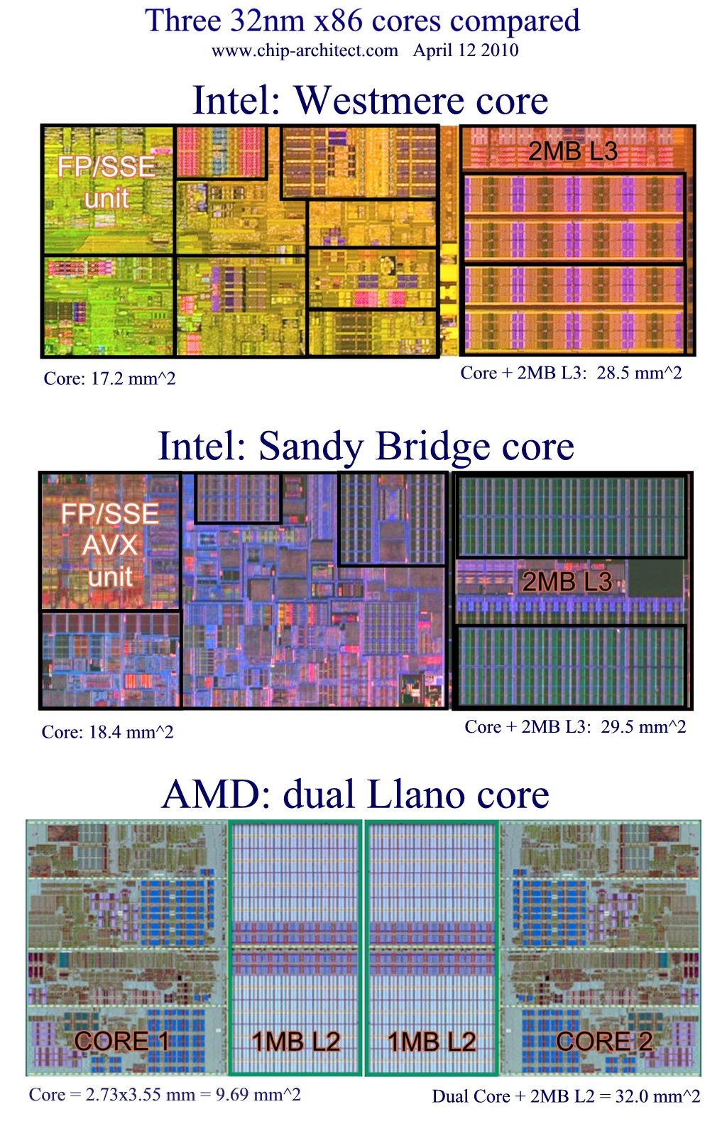
- ^ (JPEG) Llano vs Sandy Bridge vs Westmere, Chip Architect, http://www.chip-architect.com/news/Llano_vs_SandyBridge_vs_Westmere.jpg
- ^ List of Intel Mobile Core i7 Extreme processor, Intel, http://ark.intel.com/ProductCollection.aspx?familyID=43403&MarketSegment=MBL
- ^ Shilov, Anton (2010-04-13), Intel Begins to Ship Samples of Sandy Bridge amid Superior 32nm Production Ramp. Intel: Our 32 nm Production Ramp – Fastest Ramping Process Ever, X Bit Labs, http://www.xbitlabs.com/news/cpu/display/20100413235813_Intel_Begins_to_Ship_Samples_of_Sandy_Bridge_amid_Superior_32nm_Production_Ramp.html
- ^ http://en.inpai.com.cn/doc/enshowcont.asp?id=7947&pageid=7714
- ^ http://www.anandtech.com/show/4083/the-sandy-bridge-review-intel-core-i7-2600k-i5-2500k-core-i3-2100-tested/11
- ^ Intel to limit Sandy Bridge Overclocking, Bit-Tech, July 22, 2010, http://www.bit-tech.net/news/hardware/2010/07/22/intel-to-limit-sandy-bridge-overclocking/1
- ^ Anand Lal Shimpi (2010-09-14). "Intel’s Sandy Bridge Architecture Exposed". AnandTech. p. 8. http://www.anandtech.com/show/3922/intels-sandy-bridge-architecture-exposed/8. Retrieved 2010-12-16.
- ^ http://www.youtube.com/watch?v=hKGnaTrxS_k
- ^ "IDF Intel 2010: Intel Overclocks Sandy Bridge CPU to 4.9 GHz, outpaces 12-core AMD Opteron". ZDNet. http://www.zdnet.com/blog/computers/idf-intel-2010-intel-overclocks-sandy-bridge-cpu-to-49ghz-outpaces-12-core-amd-opteron/3863.
- ^ "Intel Sandy Bridge E Processors to Come with Unlocked Base Clock - Softpedia". News.softpedia.com. http://news.softpedia.com/news/Intel-Sandy-Bridge-E-Processors-to-Comes-with-Unlocked-Base-Clock-169024.shtml. Retrieved 2010-12-05.
- ^ http://www.overclock.net/intel-general/890563-15-days-till-sandy-bridge-released.html
- ^ http://img697.imageshack.us/img697/2337/4600.jpg
- ^ Jason Cross (March 17, 2008). "Intel Offers Peek at Nehalem and Larrabee". ExtremeTech. http://www.extremetech.com/article2/0,1697,2276802,00.asp.
- ^ Intel IDF Preview: Tukwilla, Dunnington, Nehalem and Larrabee, PC Per, http://www.pcper.com/article.php?aid=534&type=expert&pid=3
- ^ Gruener, Wolfgang (14th Aug 2008), Leaked IDF slides shed light on Nehalem’s successors, TG Daily, http://www.tgdaily.com/content/view/38891/135/
- ^ Knupffer, Nick. "Intel Insider - What Is It? (IS it DRM? And yes it delivers top quality movies to your PC)". http://blogs.intel.com/technology/2011/01/intel_insider_-_what_is_it_no.php. Retrieved 2011-02-02.
- ^ Hachman, Mark (2010-09-14). "Intel’s ‘Sandy Bridge’ Chip to Include vPro Business Features". PC Magazine. http://www.pcmag.com/article2/0,2817,2369110,00.asp.
- ^ Tom's Hardware,Intel Identifies Cougar Point Chipset Error, Halts Shipments http://www.tomshardware.com/news/cougar-point-sandy-bridge-sata-error,12108.html
- ^ Intel Corporation (January 31, 2011). "Intel Identifies Chipset Design Error, Implementing Solution". Press release. http://newsroom.intel.com/community/intel_newsroom/blog/2011/01/31/intel-identifies-chipset-design-error-implementing-solution.
- ^ http://www.bbc.co.uk/news/technology-12354263
- ^ http://abcnews.go.com/Business/wireStory?id=12825978
- ^ http://www.reuters.com/article/2011/02/02/uk-intel-hp-idUKTRE7118OL20110202
- ^ http://www.pcmag.com/article2/0,2817,2379241,00.asp
- ^ http://www.pcworld.com/article/218919/intel_to_ship_dualcore_sandy_bridge_chips_on_feb_20.html
- ^ (in Japanese) (Encoding: EUC-JP) “SandyBridge”世代のデスクトップCPU, 北森瓦版 / northwood.blog60.fc2.com, 2009-11-27, http://northwood.blog60.fc2.com/blog-entry-3318.html, retrieved 2010-12-16, English translation.
- ^ Kaigai; Hiroshige Goto (2010-03-01), "32nmプロセス世代のIntelとAMDのCPU" (in Japanese) (Encoding: SHIFT_JIS), PC Watch (Japan: Impress Watch), http://pc.watch.impress.co.jp/docs/column/kaigai/20100301_351592.html, retrieved 2010-12-16, English translation.
- ^ Kaigai; Hiroshige Goto (2010-04-09), "ノートPCからMPサーバーまで投入されるIntelの「Sandy Bridge」" (in Japanese) (Encoding: SHIFT_JIS), PC Watch (Japan: Impress Watch), http://pc.watch.impress.co.jp/docs/column/kaigai/20100409_360112.html, retrieved 2010-12-16, English translation.
- ^ a b c d Swinburne, Richard (2010-04-21). "Intel Sandy Bridge: Details of the next gen". bit-tech. http://www.bit-tech.net/hardware/cpus/2010/04/21/intel-sandy-bridge-details-of-the-next-gen/1. Retrieved 2010-12-16.
- ^ a b c Galistel, Andreas (2010-08-09). "Sandy Bridge-E LGA 2011 socket pictured". NordicHardware. http://www.nordichardware.com/news/69-cpu--chipset/40764-sandy-bridge-e-lga-2011-socket-pictured.html. Retrieved 2010-12-16.
- ^ a b c Lal Shimpi, Anand (2010-08-27). "The Sandy Bridge Preview". AnandTech. http://www.anandtech.com/show/3871/the-sandy-bridge-preview-three-wins-in-a-row/3. Retrieved 2010-12-16.
- ^ http://www.brightsideofnews.com/news/2010/8/7/sandy-bridge-socket-pictures-leak.aspx
- ^ http://www.overclockers.com/intel-replace-lga1366-socket-2011/
- ^ Sandy Bridge Sockets, Hiroshige Goto
- ^ (in German) Neue Roadmap: „Sandy Bridge“ entschlüsselt (Update 2), Hardware News, ComputerBase, 11.08.2010, http://www.computerbase.de/news/hardware/prozessoren/intel/2010/august/neue_intel_cpu-roadmap_sandy_bridge/, English translation.
- ^ (in Chinese), Ex Preview, http://www.expreview.com/11683.html, English translation.
- ^ "Price And Release Day Of Intel Sandy Bridge Processor Confirmed - Expreview.com". En.expreview.com. http://en.expreview.com/2010/11/26/price-and-release-day-of-intel-sandy-bridge-processor-confirmed/12357.html. Retrieved 2010-12-05.
- ^ a b c "Intel's Sandy Bridge E-Series in Q4 2011". Tom's Hardware. 2011-02-11. http://www.tomshardware.com/news/Sandy-Bridge-E-Series-Patsburg-Direct-Media-Interface-Core-i7-9-series,12179.html. Retrieved 2011-02-13.
- ^ a b "The Sandy Bridge Review: Intel Core i7-2600K, i5-2500K and Core i3-2100 Tested". Anandtech. 2011-01-03. http://www.anandtech.com/show/4083/the-sandy-bridge-review-intel-core-i7-2600k-i5-2500k-core-i3-2100-tested/6. Retrieved 2011-02-13.
- ^ http://www.semiaccurate.com/2010/10/06/more-sandy-bridge-details-leak/
- ^ http://www.semiaccurate.com/2010/10/06/sandy-bride-xeon-model-numbers-explained/
- ^ News, Digitimes, 2010-11-15, http://www.digitimes.com/news/a20101115PD211.html
- ^ Intel low power embedded Sandy Bridge coming in Q1'11, Semiaccurate, 2010-10-12, http://www.semiaccurate.com/2010/10/12/intel-low-power-embedded-sandy-bridge-coming-q111/
- ^ http://www.anandtech.com/show/4084/intels-sandy-bridge-upheaval-in-the-mobile-landscape
- ^ Burt, Jeffrey (2010-09-17). "Intel Plans for 22-nm 'Ivy Bridge,' 15-nm Atom Chips". eWeek. http://www.eweek.com/c/a/Desktops-and-Notebooks/Intel-Plans-for-22nm-Ivy-Bridge-15nm-Atom-Chips-585696. Retrieved 2010-12-21.
- ^ http://vr-zone.com/articles/ivy-bridge-to-have-20-percent-performance-advantage-over-sandy-bridge/11061.html
- ^ http://vr-zone.com/articles/ivy-bridge-to-have-20-percent-performance-advantage-over-sandy-bridge/11061.html | Ivy Bridge To Have 20 percent performance advantage
- ^ http://www.nordichardware.com/news/69-cpu-chipset/42215-ivy-bridge-graphics-gets-16-eus-and-directx-11.html
- ^ http://www.fudzilla.com/graphics/item/21658-16-graphics-eus-in-ivy-bridge
- ^ http://tech2.in.com/india/news/cpus/is-intel-making-ivy-bridge-backwards-compatible/194222/0
- ^ http://www.funkykit.com/pc-tech/7357-intel-to-unveil-22nm-ivy-bridge-cpus-at-computex-2011.html
External links
- Intel's AVX page
- Marco Chiappetta (January 02, 2011). "Intel Core i7-2600K and i5-2500K Processors Debut". HotHardware.com. http://hothardware.com/Reviews/Intel-Core-i72600K-and-i52500K-Processors-Debut/. Retrieved January 02, 2011.
- David Kanter (September 25, 2010). "Intel's Sandy Bridge Microarchitecture". realworldtech.com. http://www.realworldtech.com/page.cfm?ArticleID=RWT091810191937&p=1. Retrieved December 16, 2010.
- Anand Lal Shimpi (September 14, 2010). "Intel's Sandy Bridge Architecture Exposed". anandtech.com. http://www.anandtech.com/show/3922/intels-sandy-bridge-architecture-exposed/1. Retrieved December 16, 2010.
- Gabriel Torres (December 30, 2010). "Inside the Intel Sandy Bridge Microarchitecture". hardwaresecrets.com. http://www.hardwaresecrets.com/article/Inside-the-Intel-Sandy-Bridge-Microarchitecture/1161/1. Retrieved January 16, 2011.
- Andrew Van Til (January 3, 2011). "Intel Sandy Bridge: Core i5-2500K and DH67BL Motherboard". www.missingremote.com. http://www.missingremote.com/review/intel-sandy-bridge-core-i5-2500k-and-dh67bl-motherboard. Retrieved January 3, 2011.
- Inside the Intel Sandy Bridge Microarchitecture
| ||||||||||||||||||||||||||||||||||||||||||||||||||||||||||||||||||||||||||||||||||||||||||||||||||||||||||||||||||||||||||||||||||||||
No comments:
Post a Comment